
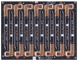
800G Optical Module PCB: The Core Foundation for AI Data Center High-Speed Interconnection
May 15, 2026
The explosive growth of AI large-model computing power is accelerating the iteration of data center optical communication technology from 400G to 800G. In 2025, global 800G optical module shipments rose by 60% year-on-year. As the "physical core" of optical modules, PCBs serve as the critical carrier for 112Gbps per-channel high-speed transmission, high-density integration, and efficient heat dissipation.
Unlike conventional circuit boards, 800G optical module PCBs are high-end electronic substrates integrating ultra-low loss materials, HDI high-density interconnection, precise impedance control, and efficient thermal design — all of which directly determine the signal integrity, stability, and service life of optical modules.
1. Core Pain Points: The Technical Gap Between 400G and 800G PCBs
Mainstream 800G optical modules (QSFP-DD/OSFP packaging) feature comprehensive upgrades in speed, density, and power consumption, rendering traditional PCB processes obsolete. Below are the four key technical bottlenecks:
-
Severe Signal Loss & Uncontrolled Bit Error Rate: With a single-channel rate of 112Gbps (PAM4 encoding) and a Nyquist frequency of 56GHz, conventional FR-4 materials (Df≥0.01) cause insertion loss of up to -1.5dB/inch, resulting in a bit error rate (BER) exceeding 10⁻⁷ — far above the commercial standard of ≤10⁻¹².
-
High-Density Wiring Dilemma & Severe Crosstalk: QSFP-DD packaging doubles the pin count. Traditional through-holes (≥0.2mm) take up excessive space, requiring line width/spacing to shrink to below 0.1mm. Wiring density jumps from 120 points/cm² to 200 points/cm², increasing crosstalk to above -60dB.
-
High Power Consumption & Heat Dissipation Challenges: 800G optical modules consume 15-20W of power, with laser and driver chips reaching a power density of 2W/cm². Conventional FR-4 (thermal conductivity: 0.3W/(m·K)) causes chip junction temperatures to exceed 80℃, reducing output power by 15% and shortening service life by 50%.
-
Insufficient Reliability & Low Mass Production Yield: Modules require stable operation between -40℃ and 125℃. Traditional through-hole solder joints are prone to cracking due to thermal expansion and contraction, with hole position deviations of ±0.05mm, leading to a mass production yield of less than 60%.
2. Four Core Technical Breakthroughs for 800G PCBs
2.1 Ultra-Low Loss Materials: The "Expressway" for High-Speed Signals
Materials are the foundation of 800G PCBs, requiring low Dk (dielectric constant), low Df (dissipation factor), high Tg, and thermal stability. Mainstream materials fall into three categories:
|
Material Category
|
Representative Products
|
Dk (@10GHz)
|
Df (@10GHz)
|
Application Scenario
|
|---|---|---|---|---|
|
High-End High-Speed
|
Panasonic Meg7/M7N, Shengyi S7439, Rogers RO4835
|
3.0~3.6
|
≤0.003
|
Critical signal layers (112Gbps PAM4)
|
|
Mid-End Hybrid
|
Low-Loss FR-4 (e.g., Taiguang EM-888K)
|
4.0~4.5
|
0.005~0.008
|
Non-critical signal layers (cost balance)
|
|
Heat Dissipation-Enhanced
|
AlN Ceramic Substrate, Aluminum-Based Heavy Copper
|
N/A
|
N/A
|
High-power chip areas
|
2.2 HDI High-Density Interconnection: Key to Miniaturization & High Speed
800G PCBs primarily adopt a12-14 layer Anylayer HDI structure (3+N+3 third-order), with laser blind/buried vias replacing traditional through-holes to address density challenges:
-
Microvia Processing: UV laser drilling creates vias with diameters of 0.075-0.15mm (minimum 0.05mm) and hole wall roughness of Ra≤1.5μm (vs. industry standard 3μm).
-
Blind/Buried Via Design: Blind vias connect surface and inner layers; buried vias connect inner layers without penetrating the entire board. This design increases wiring density by 50%, shortens signal paths by 30%, and reduces parasitic inductance/capacitance by 40%.
-
Stack-Up Specifications: Board thickness of 0.6-1.0mm, warpage ≤0.5%; a complete, unsegmented ground plane; differential pairs referenced on the same layer; impedance controlled at 50Ω (single-ended) / 100Ω (differential) ±5%.
2.3 Precision Signal Integrity Control: Eliminating Bit Errors
112Gbps PAM4 signals demand strict control over impedance, length, and shielding. Three key control points:
-
Accurate Impedance Control: LDI (Laser Direct Imaging) achieves a line width tolerance of ±0.02mm and impedance fluctuation <5%. TDR (Time Domain Reflectometry) scanners perform full-board testing to locate impedance mutation points with ±1Ω accuracy.
-
Differential Pair Matching: Differential line width/spacing of 0.08mm; length mismatch within the same pair ≤5μm, and between pairs ≤20μm; crosstalk suppressed to below -100dB.
-
Multi-Layer Shielding: Alternating stack-up of signal, ground, and power layers (inner copper: 25μm; outer copper: 35μm) reduces electromagnetic interference (EMI).
2.4 Efficient Thermal Dissipation & Reliability Design
To ensure long-term stable operation, 800G PCBs integrate targeted thermal and reliability features:
-
Vertical Heat Dissipation Channel: A combination of blind/buried vias and heavy copper (10oz) creates a path from chip → surface copper → blind via → inner ground plane → PCB bottom, improving thermal conductivity by 40% and keeping chip junction temperatures below 60℃.
-
Surface Finish: ENEPIG or immersion gold + thick gold plating (gold finger thickness: 0.1-0.2μm) supports over 500 insertions/extractions. Bonding pads (75μm×75μm, ±3μm tolerance) enhance bonding strength by 20%.
-
Wide-Temperature Reliability: High Tg materials (Tg≥280℃) with CTE ≤12ppm/℃ pass 1000 thermal cycles (-40℃~125℃) without solder joint cracking.
3. Typical Specifications & Mass Production Critical Controls
3.1 Core Specifications
|
Item
|
Mainstream Specification
|
Remarks
|
|---|---|---|
|
Layer Count
|
12-14 Layers AnyLayer
|
High-end: 14-layer 3-order HDI
|
|
Base Material
|
Meg7N/RO4835 + Low-Loss FR-4
|
Hybrid lamination for performance-cost balance
|
|
Min Line Width/Spacing
|
0.07-0.1mm / 0.07-0.1mm
|
LDI process, ±0.02mm tolerance
|
|
Blind Via Diameter
|
0.075-0.1mm
|
Laser drilling, 1:10 aspect ratio
|
|
Impedance Control
|
Single-ended 50Ω±5%; Differential 100Ω±5%
|
Full high-frequency testing
|
|
Board Thickness/Warpage
|
1.0mm±0.1mm; ≤0.5%
|
Ultra-thin, high flatness
|
|
Surface Finish
|
ENEPIG / Immersion Gold + Thick Gold
|
Compatible with wire bonding & SMT
|
3.2 Mass Production Key Controls
-
Base Material Processing: High-frequency materials are brittle and fluorine-containing; use diamond-coated drill bits at 30000-40000rpm to ensure hole wall roughness ≤1.5μm.
-
Lamination Process: Multi-layer lamination at 220-250℃ and 15-20kg/cm², with layer thickness uniformity deviation ≤±5%.
-
Inspection Standards: Terahertz AOI for defect detection, full impedance testing, and full differential length matching inspection to ensure mass production yield ≥85%.
4. Industry Trend: From 800G to 1.6T, Continuous PCB Iteration
As AI computing demand continues to surge, optical modules are rapidly evolving from 800G to 1.6T, driving synchronous PCB upgrades:
-
More Layers: 1.6T PCBs will feature 14-16 layers with a 7-2-7 Anylayer structure, increasing wiring density by an additional 30%.
-
Material Upgrade: Next-generation materials (e.g., Meg8, Rogers RO4000 series) with Dk≤3.0 and Df≤0.002 will support 200Gbps per-channel transmission.
-
Process Innovation: Laser Direct Etching (LDE) and nano-scale surface treatment will shrink line width/spacing to 0.05mm, with impedance tolerance tightened to ±3%.
-
Accelerated Domestic Substitution: Chinese manufacturers (Shengyi, Taiguang, Shennan Circuits) have broken overseas monopolies in Meg7-level materials and 14-layer AnyLayer technology, reducing costs by 20-30%.
5. Conclusion
800G optical module PCBs are core strategic components for AI data center high-speed interconnection. Their technological breakthroughs rely on the ultimate synergy of materials, processes, and design. From ultra-low loss materials to HDI interconnection, and from precise signal integrity control to efficient thermal design, every technical detail directly impacts optical module performance and reliability.
With the volume shipment of 800G modules and the R&D of 1.6T technology, the PCB industry is entering a new growth cycle. For PCB manufacturers, mastering three core capabilities — high-frequency low-loss material processing, Anylayer HDI, and precise signal integrity control — is critical to seizing opportunities in the high-speed optical communication market. For optical module and data center customers, partnering with technically mature, high-yield PCB suppliers is key to maintaining product competitiveness.

800G Optical Module PCB: The Core Foundation for AI Data Center High-Speed Interconnection
May 15, 2026

77GHz Millimeter-Wave Radar PCB: Unlocking Performance with RO3003+FR4 Hybrid Lamination
May 05, 2026
.jpg)
Computer Mainboard & Computer System Motherboard Manufacturing for OEM & Industrial Applications
Feb 18, 2026
CPU Fan in Motherboard Design, CPU Front Panel Integration & PCB Manufacturing Standards
Feb 11, 2026
10 years of dedicating to PCB manufacturing
Provide your email or phone number, and our sales engineer will reach out soon with a professional quotation.